Materials & Methods
Materials
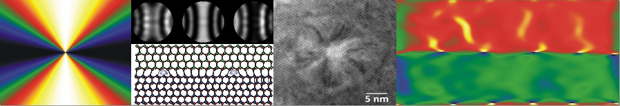
- Polycrystalline Silicon
- Cubic & Hexagonal Symmetry Metals
- Magnetic Materials
- Ceramics
- Amorphous Metal Glasses
- Glasses and Glass-Ceramic Materials for Vitrification and Waste Management
- Multilayer Silicon Structures
- Low Dimensional III-V Semiconductors (Quantum Wells, Nanowires, Quantum Dots)
Methods
- Conventional Transmission Electron Microscopy (CTEM) combined with Selected Area Electron Diffraction (SAED) providing information on the overall structural quality, defect content and the orientation relationship of epitaxial structures
- High Resolution TEM (HRTEM) for the local atomic arrangement of interfacial and defect structures
- Local atomic chemistry of nanostructures idenitified by High Angle Annular Dark Field (HAADF) imaging, Energy Dispersive X-ray Spectroscopy (EDX) and Electron Energy Loss Spectroscopy (EELS)
- Topological analysis for a priori characterization of line and extended defects
- Quantitative HRTEM (qHRTEM) image processing techniques (Geometrical Phase Analysis, peak finding and projection method)
- Large scale energetic calculations of atomic structures with empirical potentials (Molecular Dynamics)
- Structural and optoelectronic properties of semiconductors based on first principles calculations (Density Functional Theory, DFT)
- Utilization of the “Vitrification” for the stabilization-solidification of inorganic toxic wastes